1. Introduction: The Rise of Wide Bandgap (WBG) Semiconductors
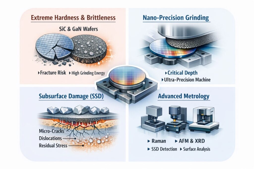
The semiconductor industry is undergoing a paradigm shift from traditional Silicon (Si) to Wide Bandgap (WBG) materials, specifically Silicon Carbide (SiC) and Gallium Nitride (GaN). These materials are essential for the next generation of power electronics, electric vehicles (EVs), and 5G infrastructure due to their ability to operate at higher voltages, temperatures, and frequencies. However, the very properties that make them electrically superior—extreme hardness and chemical inertness—make them notoriously difficult to machine.
The Hardness Barrier
SiC, in particular, is one of the hardest known materials, with a Mohs hardness of approximately 9.5 (approaching that of diamond). In comparison to standard Silicon, SiC is significantly more brittle and possesses a high Specific Grinding Energy. Traditional grinding methods that work for Si wafers lead to catastrophic fracture, edge chipping, and severe subsurface damage when applied to SiC. For GaN, which is often grown as a thin epitaxial layer on sapphire or SiC substrates, the challenge lies in the mismatch of mechanical properties between the layer and the substrate during the thinning process.
Wafer Thinning and Yield Economics
To maximize the thermal and electrical efficiency of power devices, the wafers must be thinned down to thicknesses of 100 μm or less. This Back-grinding process is the single most risky step in wafer fabrication. A single micro-crack induced during grinding can propagate during subsequent thermal processing, leading to the loss of an entire wafer worth tens of thousands of dollars. Therefore, the grinding process must transition from “material removal” to Damage-Free Surface Generation.
The fundamental challenge is to remove material at a productive rate without inducing brittle fracture. To solve this, we must look at the nanoscopic physics of the contact zone. In the next section, we explore Ductile-to-Brittle Transition: The Physics of “Nano-grinding”.
From a fab perspective, this is where mechanical engineering quietly becomes a yield lever. A few nanometers of hidden damage can dictate whether the wafer survives the next thermal step—or turns into scrap.
2. Ductile-to-Brittle Transition: The Physics of “Nano-grinding”
The traditional understanding of grinding brittle materials like SiC and GaN involves microscopic chipping and crack propagation. However, when the depth of cut per grit is reduced below a certain threshold, even the most brittle ceramic undergoes a Ductile-to-Brittle Transition. In this “Ductile Mode,” the material is removed via plastic flow rather than fracture, resulting in a mirror-like finish with significantly reduced subsurface damage.
The Critical Depth of Cut (dc)
To achieve ductile-mode grinding, the uncut chip thickness must be kept below a critical value, dc. This value is a function of the material’s intrinsic properties: its Fracture Toughness (Kc), Hardness (H), and Elastic Modulus (E). For SiC, this critical depth is typically in the range of 10 to 100 nanometers. If the grinding grit penetrates deeper than this, the energy exceeds the threshold for plastic deformation and triggers lateral and median cracks.
Nanoscopic Material Removal Mechanism
In the ductile regime, the diamond grit acts as a microscopic plow. The high hydrostatic pressure generated at the extremely sharp grit tip suppresses crack initiation and allows the crystalline lattice of the SiC or GaN to “flow” around the tool. This process is often called Nano-grinding because it requires machine tools with sub-micron positioning accuracy to maintain the chip thickness within this ultra-thin window.
The Role of Specific Energy in Phase Transformation
Ductile grinding requires extremely high Specific Energy (u) because the material is being sheared at a near-atomic level. This energy can sometimes induce localized phase transformations in SiC, turning the crystalline structure amorphous. While this suppresses cracking, it creates a new challenge: a “damaged” amorphous layer that must be characterized.
This tendency becomes more relevant under high local flash temperature and sustained contact, especially when the wheel begins to dull.
Understanding how to stay within this ductile window is the only way to protect the wafer’s integrity. In the next section, we dive deeper into the consequences of failing to maintain this balance: Subsurface Damage (SSD): The Hidden Yield Killer.
3. Subsurface Damage (SSD): The Hidden Yield Killer
In semiconductor manufacturing, the “mirror finish” achieved on the surface of a SiC wafer can be deceptive. Beneath the polished exterior often lies a network of Micro-cracks, Dislocations, and Residual Stresses. This is known as Subsurface Damage (SSD). For WBG materials, SSD is the primary cause of wafer breakage during downstream thermal processes and the leading driver of electrical leakage in finished power devices.
The Hierarchy of SSD: Cracks to Dislocations
SSD in SiC typically manifests in two layers. The upper layer consists of Median and Lateral Cracks caused by brittle fracture. Below this lies a deeper zone of Crystalline Lattice Distortion and plastic deformation. While the cracks might be removed during the initial CMP (Chemical Mechanical Polishing) stages, the deeper lattice dislocations can act as “nucleation sites” for further defects during epitaxial growth, effectively ruining the wafer’s electrical performance.
The “1-to-10” Rule of Damage Depth
A common rule of thumb in semiconductor grinding is that the depth of SSD is approximately 1 to 10 times the peak-to-valley surface roughness (Rt). However, for SiC, the high hardness can cause Deep Median Cracks that extend far beyond this ratio if the grinding force is not strictly controlled. If the SSD depth exceeds the intended material removal of the subsequent CMP process, the “hidden” damage remains, leading to catastrophic yield loss in the final fab stages.
The Economics of SSD Removal
Every micron of SSD that must be removed via CMP represents a massive increase in manufacturing cost, as CMP is significantly slower and more expensive than grinding. The goal of advanced Back-grinding is to minimize the SSD depth to a level that can be cleared in a single, rapid polishing pass. This requires a shift toward the specific tool and bond technologies discussed in the next section.
To control this invisible enemy, we must choose our weapons wisely. In the next section, we examine Section 4: Diamond Tooling Strategies: Grit Size and Bond Chemistry.
4. Diamond Tooling Strategies: Grit Size and Bond Chemistry
Grinding SiC and GaN wafers is a battle of attrition against extreme hardness. Conventional abrasives like Alumina or Silicon Carbide are useless here, as their hardness is too close to the workpiece itself. Diamond is the only viable abrasive, but its effectiveness depends entirely on the Grit Size and the Bond Chemistry that holds it. For WBG semiconductors, the strategy must shift from “aggressive removal” to “controlled nanoscopic cutting.”
Sub-micron Grit Selection
To maintain the Ductile Mode discussed in Section 2, the abrasive grains must be extremely small. While rough grinding of SiC ingots might use #200 to #400 mesh diamond, wafer back-grinding requires Fine Diamond Grits ranging from #2000 to #8000 (average grain size of 1 to 5 μm). Smaller grits increase the number of active cutting points, thereby reducing the force per grit and keeping the uncut chip thickness below the critical brittle-to-ductile transition threshold.
Vitrified vs. Resin Bonds: The Stiffness Conflict
The bond material determines how the wheel behaves under load. Vitrified Bonds (ceramic-based) offer high stiffness and excellent thermal stability, which is essential for maintaining the flat “topography” of the wafer. However, their rigidity can lead to high impact forces. Resin Bonds provide a degree of “cushioning” that absorbs micro-vibrations, making them ideal for the final finishing stages where minimizing SSD is the priority. Many modern SiC processes utilize a Hybrid Bond that combines the stiffness of vitrified with the resilience of resin.
The “Self-Sharpening” Requirement
SiC grinding generates high temperatures that can cause diamond graphitization (the reversion of diamond back to carbon). To combat this, the bond must be designed for Controlled Erosion. As the diamond grits dull, the bond must wear away at a precise rate to expose fresh, sharp cutting edges. If the bond is too hard, the wheel will “glaze,” leading to massive friction and wafer thermal cracking (warpage).
Even the best tool is useless without a machine capable of nanometer-level control. In the next section, we examine Section 5: Precision Machine Dynamics: Nanometer-level Infeed Control.
5. Precision Machine Dynamics: Nanometer-level Infeed Control
To maintain the Ductile Mode grinding window, the machine tool must exhibit extreme static and dynamic stiffness. In semiconductor back-grinding, where we deal with ultra-thin wafers (often down to 100 μm), even a vibration of a few hundred nanometers can cause the diamond grit to exceed the critical depth of cut, triggering brittle fracture and ruining the entire batch.
Air Bearing Spindles and Vibration Damping
High-precision back-grinders utilize Air Bearing Spindles to eliminate the mechanical noise associated with ball bearings. These spindles provide near-zero friction and exceptional rotational accuracy. Furthermore, the machine bed is often constructed from Synthetic Granite or epoxy composites, which offer significantly higher damping ratios than cast iron, absorbing the high-frequency harmonics generated during the high-speed grinding of hard SiC.
Constant Infeed vs. Constant Pressure
For Silicon, constant pressure grinding is common. However, for SiC and GaN, a Deterministic Infeed Control strategy is mandatory. The machine must feed the wheel at a constant, infinitesimal rate (e.g., 0.1 to 0.5 μm/sec). This ensures that the material removal rate is driven by the machine’s precision rather than the material’s varying resistance, preventing “surges” in force that lead to SSD.
In practice, the achievable stability is constrained by chuck vacuum uniformity, wheel wear state, and thermal drift—so targets should be set with these on-tool limits in mind.
TTV (Total Thickness Variation) Control
The mechanical alignment between the spindle and the porous ceramic chuck (which holds the wafer via vacuum) must be perfect. Any angular misalignment leads to a “wedge” shape, resulting in high TTV. In SiC power devices, TTV is critical because it directly affects the thermal dissipation path; an uneven wafer creates “hot spots” that reduce the device’s lifespan.
While machine dynamics provide the stability, the interaction between the chemistry of the fluid and the material surface provides the final edge. In the next section, we examine Section 6: Chemical-Mechanical Synergy: Advanced Slurry & Fluid Interaction.
6. Chemical-Mechanical Synergy: Advanced Slurry & Fluid Interaction
As we push for higher throughput in SiC and GaN manufacturing, pure mechanical grinding often reaches its physical limit. To overcome the extreme hardness of these materials, modern processes utilize Chemical-Mechanical Synergy. By introducing chemically active agents into the grinding fluid, we can temporarily “soften” the wafer surface, allowing for faster removal rates with lower mechanical force.
Surface Softening through Oxidation
SiC is chemically inert, but under high local temperatures and specific pH conditions, it can form a thin Hydrated Silicon Oxide (SiO2) layer. This oxide layer is significantly softer than the parent SiC crystal. Advanced grinding fluids containing oxidizers (like KMnO4 or H2O2) facilitate this reaction at the contact zone. In production, the chemistry is selected conservatively for material compatibility, corrosion control, and waste handling rather than pure removal rate. The diamond grit then removes the soft oxide layer, effectively “peeling” the wafer at a molecular level rather than fracturing the hard bulk.
Thermal Management & Warpage Prevention
For thinned wafers (especially GaN-on-Si), thermal control is critical to prevent Wafer Warpage. The grinding fluid must have high convective cooling capacity to manage the high specific energy of WBG grinding. If the temperature gradient across the wafer diameter exceeds a few degrees, the resulting internal stresses can cause the wafer to “potato chip,” making it impossible to hold flat on the vacuum chuck for the final CMP steps.
pH Control and Waste Management
In GaN processing, the fluid’s pH must be carefully maintained to prevent uncontrolled etching of the delicate epitaxial layers. Furthermore, because SiC and diamond swarf are abrasive and chemically stable, high-efficiency Centrifugal Filtration is required to prevent the recirculating particles from scratching the mirror-like surface being generated.
Once the grinding is complete, we must prove that the surface and subsurface are within the required nanometer tolerances. In the next section, we examine Section 7: Post-Grinding Metrology: Measuring the Damage.
7. Post-Grinding Metrology: Measuring the Damage
In the world of SiC and GaN, what you cannot measure, you cannot control. Because the defects in WBG semiconductors are on a nanoscopic scale, traditional metrology tools often fall short. Validating the success of a Ductile Mode grinding process requires a suite of advanced inspection techniques that can “see” through the surface to assess the true crystal health.
Atomic Force Microscopy (AFM) & White Light Interferometry
To measure surface roughness (Ra) on thinned wafers, AFM is the gold standard, providing sub-nanometer resolution. For larger areas, White Light Interferometry (WLI) allows for rapid mapping of the wafer’s Total Thickness Variation (TTV) and bow/warp. In many high-end flows, targets are often set around sub-nanometer Ra prior to final CMP, depending on device requirements and metrology definition.
Subsurface Damage (SSD) Detection: Raman & XRD
Measuring SSD without destroying the wafer is a major challenge. Raman Spectroscopy is highly effective for SiC; changes in the Raman peak width and position indicate localized Residual Stress and lattice distortion. Similarly, X-Ray Diffraction (XRD) “Rocking Curve” analysis provides a quantitative measure of the dislocation density induced by the grinding forces. If the XRD peaks are too broad, it indicates a deep SSD layer that will likely lead to epitaxial defects.
A practical rule is to use AFM/WLI for fast surface acceptance and trend control, then escalate to Raman/XRD only when the process window shifts (new wheel, new bond, or new coolant chemistry). If yield excursions appear downstream, prioritize stress/SSD tools first—surface Ra alone can look “good” while the lattice is already compromised.
Photoluminescence (PL) Imaging
For GaN wafers, Photoluminescence Imaging is a powerful non-destructive technique. Defects and micro-cracks act as “non-radiative recombination centers,” appearing as dark spots or lines in the PL map. This allows engineers to visualize the “damage map” of the grinding process in real-time, enabling immediate adjustments to the machine’s infeed or wheel speed settings.
With these metrology insights, the path to a high-yield, high-volume production line becomes clear. In the final section, we conclude with Section 8: Conclusion: Scalability of Next-Gen Wafer Processing.
8. Conclusion: Scalability of Next-Gen Wafer Processing
The transition from Silicon to Wide Bandgap (WBG) materials like SiC and GaN is a fundamental shift in semiconductor physics, but its success hinges on the mastery of Precision Abrasive Engineering. As we have explored, the challenges of extreme hardness and brittleness are not insurmountable; they simply require a departure from traditional “brute-force” grinding toward a Deterministic, Nano-scale approach.
The Roadmap to High-Yield Manufacturing
To achieve the scalability required for the global EV and 5G markets, the grinding process must evolve into a stable, high-throughput system based on three core pillars:
- • Mastering the Ductile Window: Maintaining the uncut chip thickness (hcu) below the critical threshold to eliminate brittle fracture.
- • Intelligent Tooling: Utilizing hybrid-bonded sub-micron diamond wheels that balance rigidity with self-sharpening capabilities.
- • In-line Metrology: Integrating real-time stress and SSD monitoring (Raman, XRD) to ensure that every wafer entering CMP is of peak structural health.
The Future of WBG Machining
“The bottleneck of power electronics is no longer just the design of the circuit, but the mechanical integrity of the substrate. Precision grinding is the enabler of the WBG revolution.”
As wafer diameters move from 150 mm (6-inch) to 200 mm (8-inch) for SiC, the margins for error become even smaller. The principles of Chemical-Mechanical Synergy and Machine Stiffness established in this report will serve as the foundation for the next generation of automated, high-volume wafer fabrication facilities.
References & Further Reading
Technical Publications & Semiconductor Standards
- • Bifano, T. G., et al. (1991). Ductile-Regime Grinding: A New Technology for Machining Brittle Materials. Journal of Engineering for Industry. (The foundational paper on the $d_c$ threshold for brittle-to-ductile transition).
- • Tawakoli, T., & Azarhoushang, B. (2014). Influence of Ultrasonic Assistance on Grinding of Silicon Carbide. International Journal of Advanced Manufacturing Technology. (Focus: Reducing SSD in SiC wafers).
- • SEMI G71-0997. Specification for Backside Grinding of Silicon Wafers. (The industry standard adapted for WBG material thinning).
- • Agarwal, S., & Rao, P. V. (2008). Experimental Investigation of Surface/Subsurface Damage in Grinding of SiC. International Journal of Machine Tools and Manufacture.
Curated Internal Resources: Semiconductor Excellence
To further optimize your wafer thinning and surface preparation workflows, explore these related technical deep-dives from our primary roadmap:
GRINDING PHYSICS:
Mechanics of Grinding Forces: Understanding Tangential/Normal Forces and Force Ratio
QUALITY CONTROL:
Analysis of Sub-surface Damage: A Deterministic Evaluation of Damage Depth and Its Impact on Surface Integrity
MATERIAL COMPARISON:
Grinding Problems in Hardened Steel: Heat, Residual Stress, and Surface Damage
Metrology & Inspection Partners
- NIST (National Institute of Standards and Technology): Semiconductor Metrology Program for SSD calibration.
- Bruker Nano Surfaces: Advanced AFM and White Light Interferometry for wafer topography.
- Rigaku Corporation: X-ray diffraction (XRD) solutions for thin-film stress and dislocation density.